Designing a PCBA friendly CO2 monitor
co2mon.nz currently uses monitors based on Oliver Seiler’s open source design which I am personally building. This post describes my exploration of how to achieve production of a CO2 monitor that could enable the growth of co2mon.nz.
Goals
Primarily I want to design a CO2 monitor which allows the majority of the production process to be outsourced. In particular, the PCB should be able to be assembled in an automated fashion (PCBA).
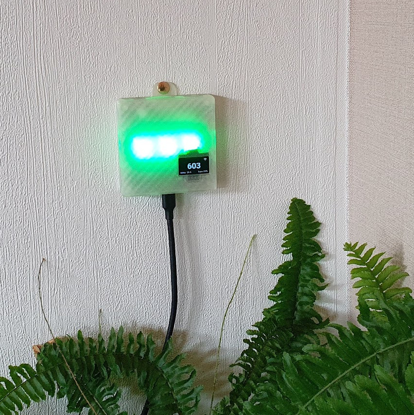
As a secondary goal, I’d like to improve the aesthetics of the monitor while retaining the unique feature of displaying clear visual indication of the current ventilation level through coloured lights.
Overall, I’ll consider the project successfull if I can achieve a visually attractive CO2 monitor which takes me less than 10 minutes per monitor to assemble/box/ship and whose production cost has the potential to be lower than the current model.
PCB
Schematic
The existing CO2 monitor design provides a solid foundation but relies upon the ESP32 Devkit board, which is intended for evaluation purposes and is not well suited to automated assembly. Replacing this devkit board with the underlying ESP32 module is the major change needed to enable PCBA production, which then also requires moving the supporting electronics from the devkit board directly onto the primary PCB.
The basic ESP32 chipset used in the devkit boards is no longer available as a discrete module suitable for placement directly onto a PCB which means the board will also have to be updated to use a more modern variant of the ESP32 chipset which is in active production such as the ESP32-S3. The ESP32-S3-WROOM1-N4 module is a very close match to the original devkit and will be suitable for this project.
In addition to the change of ESP module, I made the following other changes to the components in use:
- Added an additional temperature/humidity sensor (SHT30). The current monitors take temperature/humidity measurements from the SCD40 chipset. These are primarily intended to help in the calculation of CO2 levels and rely on an offset being subtracted to account for the heat generated by the electronic components themselves. I’ve found their accuracy to OK, but not perfect. SHT30 is a cheap part, so its addition to hopefully provide improved temperature/humidity measurement is an easy choice.
- Swapped to USB-C instead of USB-B for the power connector. USB-C is much more common than USB-B and is also smaller and not as tall off the board which provides more flexibility in the case design.
With major components selected the key task is to draw the schematic diagram describing how they electrically connect to each other, which includes all the supporting electronics (e.g. resistors, capacitors, etc) needed.
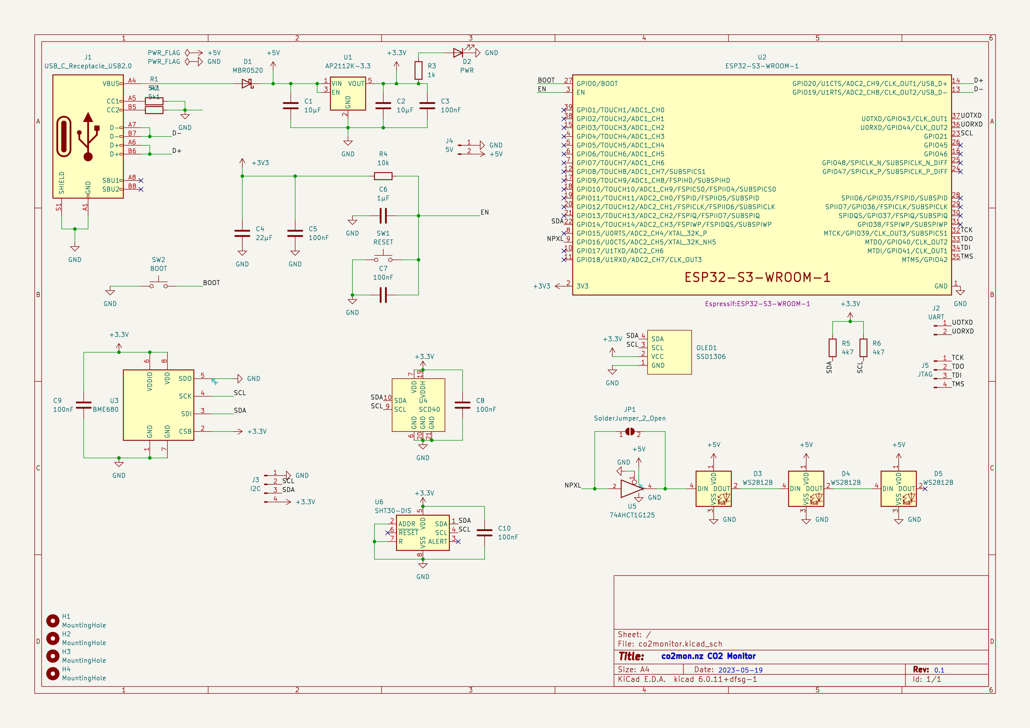
The reference design in the ESP32 datasheet (p28) and USB-C power supply examples from blnlabs were particularly helpful alongside the KiCad documentation and the example of the existing monitor in completing this step (click the image to enlarge).
Layout
The next step is to physically lay out where each component from the schematic will sit on the PCB itself. Obviously this requires first determining the overall size, shape and outline of the board and needs to occur in iteration with the intended design of the overall monitor, including the case, to ensure components like switches and USB sockets line up correctly.
In addition to the requirements around the look and function of the case, the components themselves also have considerations that must be taken into account, including:
- For best WiFi reception, the ESP32 antenna should be at the top of the monitor and should not have PCB underneath it, or for a specified distance either side of it.
- The SHT30 temperature sensor should be as far from any heat generating components (e.g. the ESP32, BME680 and SCD40 modules) as possible and also considering that any generated heat will rise, as low on the monitor as possible.
- The sensors measuring the air (SCD40, BME680 and SHT30) must have good exposure to the air outside the case.
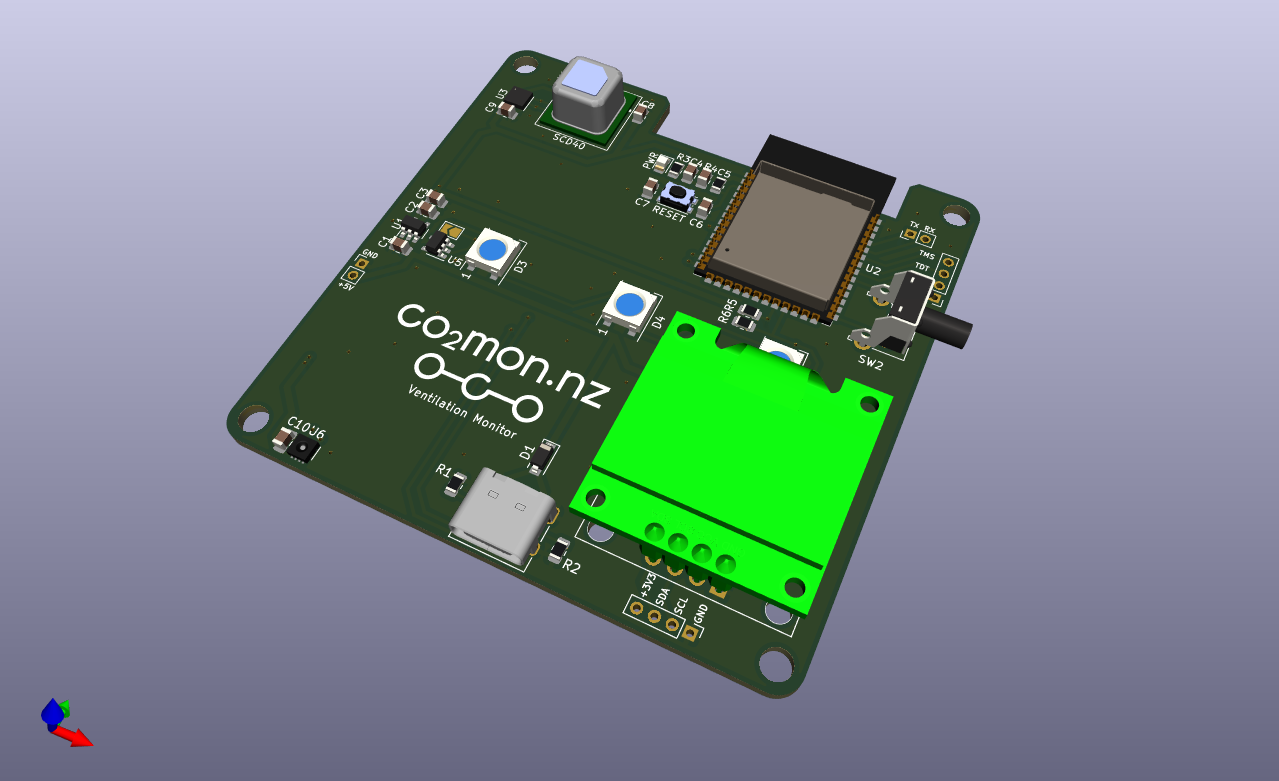
Once the components are placed, the next big task is to route the traces (aka wires) between the components on the board such that all the required electrical connections are made without any unintended connections (aka shorts) being created. This is a fun constraint solving/optimisation challenge and takes on an almost artistic aspect with other PCB designers often having strong opinions on which layout is best. The majority of the traces and routing for this board were able to be placed on the top layer of the PCB, but I also made use of the back layer for a few traces to help avoid conflicts and deal with places where different traces needed to cross each other. It’s easy to see how this step would be much more challenging and time consuming on a larger and more complex PCB design.
The final touches were to add some debugging breakouts for the serial and JTAG ports on the ESP32-S3 and a logo and various other helpful text on the silkscreen layer that will be printed on the PCB so it looks nice.
Production
For assembly of the PCB, I went with JLCPCB based out of China. The trickiest part of the process was component selection and ensuring that the parts I had planned in the schematic were available. JLCPCB in conjunction with lcsc.com provides a basic and extended part library. If you use only basic parts you get quicker and cheaper assembly, while using extended parts bumps your order into a longer process with a small fee charged for each component on the board.
Initially I spent a lot of time selecting components (particularly LEDs and switches) that were in the basic library before realising that the ESP32 modules are only available in the extended library! I think the lesson is that unless you’re building the most trivial PCB with only passive components you will almost certainly end up in the advanced assembly process anyway, so trying to stay within the basic parts library is not worth the time.
Unfortunately the SCD40 sensor, the most crucial part of the monitor, is not stocked at all by JLCPCB/LCSC! To work around this JLCPCB will maintain a personal component library for you when you ship components to them to for use in future orders. Given the extra logistical time and hassle of having to do this, combined with having a number of SCD40 components already on hand I decided to have the boards assembled without this component populated for the initial prototype run. This also had the benefit of lowering the risk if something went wrong as the cost of the SCD40 is greater than the cost of the PCB and all the other components combined!
I found the kicad-jlcpcb-tools plugin for KiCad invaluable for keeping track of what part from lcsc.com I was planning to use for each component and generating the necessary output files for JLCPCB. The plugin allows you to store these mappings in your actual schematic which is very handy. The search interface it provides is fairly clunky and I found it was often easier to search for the part I needed on lcsc.com and then just copy the part number across into the plugin’s search box rather than trying to search by name or component type.
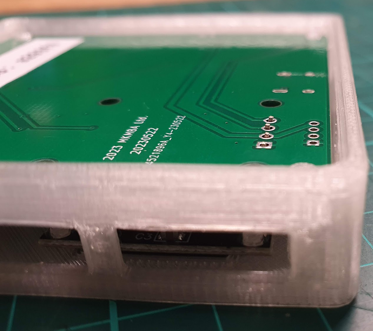
The LCD screen is the remaining component which is not easily assembled onto the PCB directly, but as you’ll see next, this actually turned out to be OK as integrating the screen directly into the case makes the final assembly process smoother.
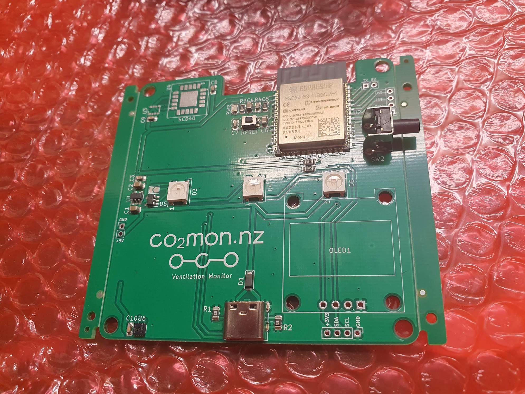
In the end there was no issue with the edge rails. The switch was placed hanging over them without issue and snapping them off once the boards arrived was a trivial 30s job using a vice to hold the edge rail and then gently tipping the board over until it snapped off - the interface between the board and the rails while solid looking has obviously been scored or perforated in some way during the production process so the edge breaks cleanly and smoothly. Magic!
The process was amazingly quick with the completed PCBs (picture above) arriving within 7 days of the order being placed and looking amazing.
Case
Design
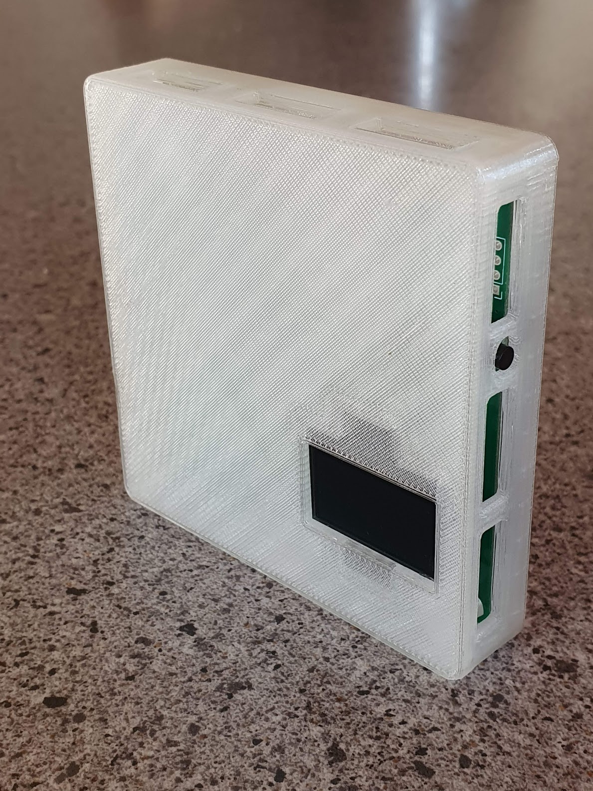
I mocked up a very simple prototype of the case in FreeCAD during the PCB design process to help position and align the placement of the screen, switch and USB socket on the PCB as all three of these components interface directly with the edges of the case. Initially this design was similar to the current monitor design where the PCB (with lights and screen attached) sits in the bottom of the case, which has walls containing grilles for airflow and then a separate transparent perspex is screwed onto the top to complete the enclosure.
As part of the aesthetic improvements for the new monitor I wanted to move away from a transparent front panel to something opaque but still translucent enough to allow the colour of the lights to show through. Without a transparent front panel the LCD also needs to be mounted directly into the case itself.
The first few prototype iterations followed the design of the original CO2 monitor with a flat front panel that attaches to the rest of the case containing the PCB, but the new requirement to also attach the LCD to the front panel proved to make this unworkable. To stay in place the LCD has to be pushed onto mounting poles containing a catch mechanism which requires a moderate amount of force and applying that force to the LCD board when it is already connected to the PCB is essentially impossible.
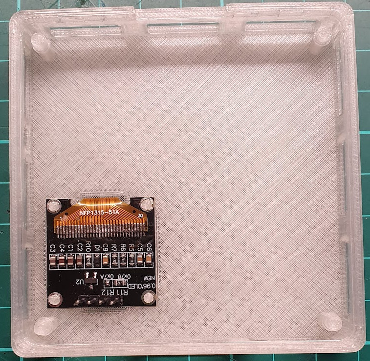
Getting to this design hugely simplified the assembly process. Starting with an empty case lying face down on a bench, the LCD screen is pushed onto the mounting poles and sits flush with the cover of the case - easily achieved without the main PCB yet in place.
Finally, a back panel can be attached which holds the PCB in place and uses “cantilever snap joints” to click on to the rest of the case.
Overall the design is a huge improvement over the previous case which required screws and spacers to position the PCB and cover relative to the rest of the case, with the spacers and screws being particularly fiddly to work with.
The major concern I had with the new design was that the mount to attach the monitor to the wall has moved from being attached to the main case and components directly to needing to be on the removable back panel - if the clips holding this panel to the case fail the core part of the monitor will fall off the wall which would not be good. To guard against this I’ve doubled the size and number of clips at the top of the case (which bears the weight) and the result seems very robust in my testing. To completely assemble a monitor, including the soldering step takes me about 2-3 minutes individually, and would be even quicker if working in batches.
Production
Given the number of design/testing iterations required to fine tune the case I chose not to outsource case production for now and used my 3D printer to produce them. I’ve successfully used JLCPCB’s 3D printing service for the previous case design, so I’m confident that getting sufficient cases printed from JLCPCB or another supplier will not be an issue now that the design is finalised.
I tried a variety of filament colours, but settled on a transparent filament which once combined in the necessary layers to form the case is not actually transparent like perspex is, but provides a nice translucent medium which achieves the goal of having the light colour visible without exposing all of the circuit board detail. There’s room for future improvement in the positioning of the LEDs on the circuit board to provide a more even distribution of light across the case but overall I really like the way the completed monitor ends up looking.
Evaluation
Building this monitor has been a really fun project, both in seeing something progress from an idea, to plans on a screen to a nice physical thing on my wall, but also in learning and developing a bunch of new skills in PCB design, assembly and 3D design.
Cost wise it’s also a huge win, primarily in terms of the time taken, but also in the raw components - currently the five prototypes I ordered and built are on par with the component cost of the original CO2 monitor, but this will drop further with larger orders due to price breaks and amortisation of the setup and shipping expenses across more monitors.
This project has also given me a much better appreciation for how much I’m only just scratching the surface of the potential complexities and challenges in producing a hardware product of this type.
I’m reasonably confident I could successfully produce a few hundred and maybe even a few thousand monitors using this approach, but it’s also clear that getting beyond that point is and would be a whole further level of effort and learning.
Hardware is hard work. That’s not news to anyone, including me, but there is something to be said for experiencing the process first hand to make the reality of what’s required real.
The PCB and case designs are both shared and can be found at https://github.com/co2monnz/co2monitor-pcb and https://github.com/co2monnz/cad, feedback and suggestions welcome!
If you liked this post and would like to receive my writing via email, please subscribe below.